找到你需要知道的一切保持韦尔斯利健康在冠状病毒(COVID-19)大流行期间。
韦尔斯利是
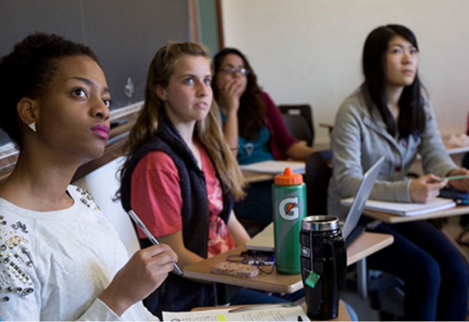
一个能激励你的地方
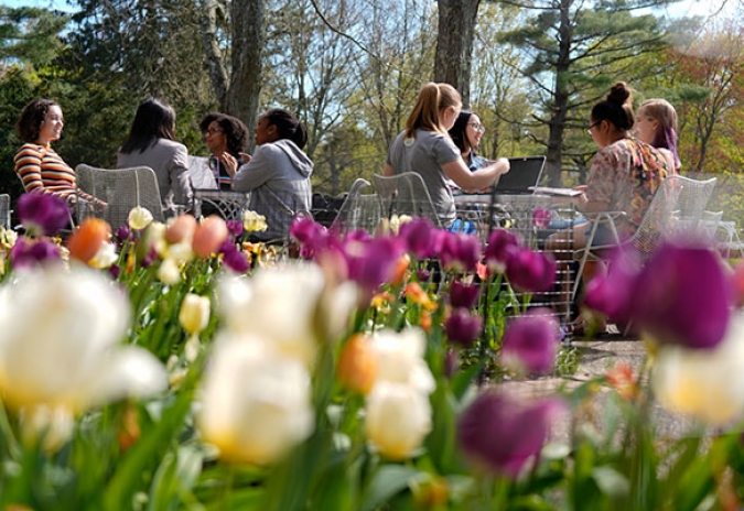
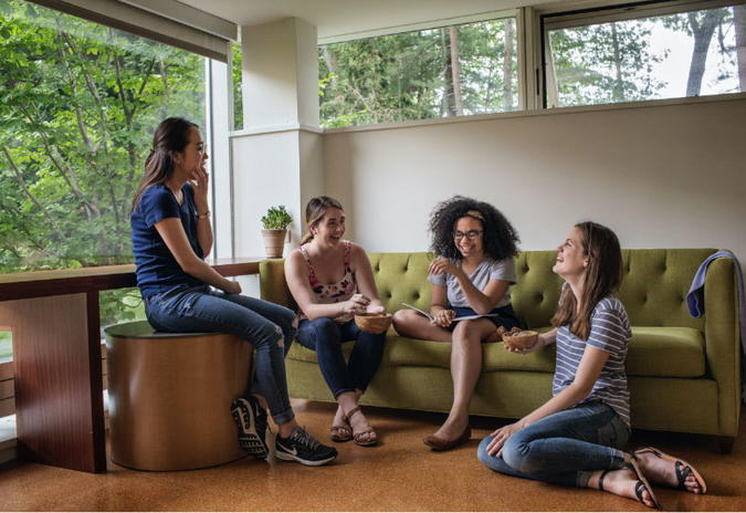
一个拥抱你的社区
一个能改变你的经历
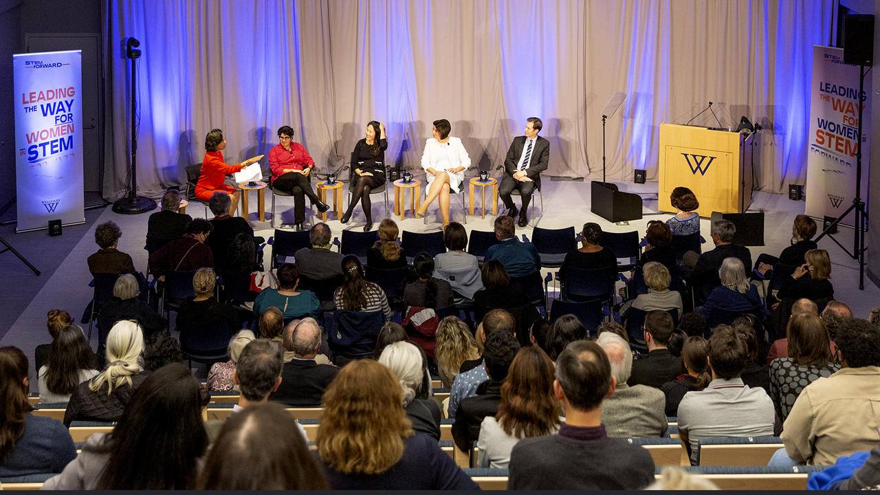
为想在世界上有所作为的女性提供优秀的文科教育
作为一名未来的学生,学习如何与卫尔斯理打交道。加上有关费用、经济援助和申请的信息。
了解我们的专业、部门、项目和语言的广度和深度。
探索校园住宿和餐饮的可能性,以及体育、健康和职业教育。
焦点集中在韦尔斯利